Fermi Energy Level In Intrinsic Semiconductor : Part I : „ position fermi energy level.. It is a thermodynamic quantity usually denoted by µ or ef for brevity. Hence, using equation 4 and rearranging, the fermi. An intrinsic semiconductor is one that contains a negligibly small amount of impurities compared with thermally note that is symmetrical around the fermi level. Room temperature intrinsic fermi level position). This means that holes in the valence band are vacancies created by electrons that we also have to know the probability for an electron to occupy a level with a given energy e.
Fermi level in intrinsic and extrinsic semiconductors. Derive the expression for the fermi level in an intrinsic semiconductor. (15) and (16) be equal at all temperatures, which yields the following expression for the position of the fermi level in an intrinsic semiconductor The probability of occupation of energy levels in valence band and conduction band is called fermi level. However as the temperature increases free electrons and holes gets generated.
pn junction - In band diagram, why the Fermi energy (EF ... from i.stack.imgur.com As the temperature increases free electrons and holes gets generated. Therefore, the fermi level for the intrinsic semiconductor lies in the middle of band gap. For notation purposes, the fermi level position in an intrinsic semiconductor is denoted as efi. Fermi level of intrinsic and extrinsic semiconductors. „ position fermi energy level. This means that holes in the valence band are vacancies created by electrons that we also have to know the probability for an electron to occupy a level with a given energy e. At this point, we should comment further on the position of the fermi level relative to the energy bands of the semiconductor. Intrinsic semiconductors are semiconductors, which do not contain impurities.
Position of fermi level in instrinsic semiconductor.
So for convenience and consistency with room temperature position, ef is placed at ei (i.e. For an intrinsic semiconductor the fermi level is exactly at the mid of the forbidden band.energy band gap for silicon (ga) is 1.6v, germanium (ge) is 0.66v, gallium arsenide (gaas) 1.424v. In intrinsic semiconductors, the fermi energy level lies exactly between valence band and conduction band.this is because it doesn't have any impurity and it is the purest form of semiconductor. Fermi level of intrinsic and extrinsic semiconductors. For an intrinsic semiconductor, every time an electron moves from the valence band to the conduction band, it leaves a hole behind in the valence band. Fermi level is dened as the energy level separating the lled states from the empty states at 0 k. Therefore, the fermi level for the intrinsic semiconductor lies in the middle of band gap. Distinction between conductors, semiconductor and insulators. Carriers concentration in intrinsic semiconductor at equilibrium. This has implications if we want to calculate $n$ and $p$, which wouldn't be equal, because they have a dependance on this energy level. The intrinsic semiconductor may be an interesting material, but the real power of semiconductor is extrinsic. Increases the fermi level should increase, is that. Fermi level in intrinsic and extrinsic semiconductors.
Above occupied levels there are unoccupied energy levels in the conduction and valence bands. Fermi level or fermi energy is a quantum phenomenon, which translates as the difference in energy state occupied by the lowest level (close to the for semiconductors (intrinsic), the fermi level is situated almost at the middle of the band gap. Room temperature intrinsic fermi level position). Solve for ef, the fermi energy is in the middle of the band gap (ec + ev)/2 plus a small correction that depends linearly on the temperature. The fermi energy or level itself is defined as that location where the probabilty of finding an occupied state (should a state exist) is equal to 1/2, that's all it is.
Energy band diagram of the CO sensor. E F is the Fermi ... from www.researchgate.net So in the semiconductors we have two energy bands conduction and valence band and if temp. For an intrinsic semiconductor, every time an electron moves from the valence band to the conduction band, it leaves a hole behind in the valence band. The probability of occupation of energy levels in valence band and conduction band is called fermi level. The distribution of electrons over a range of if the fermi energy in silicon is 0.22 ev above the valence band energy, what will be the values of n0 and p0 for silicon at t = 300 k respectively? So for convenience and consistency with room temperature position, ef is placed at ei (i.e. Those semi conductors in which impurities are not present are known as intrinsic semiconductors. The electrical conductivity of the semiconductor depends upon the total no of electrons moved to the conduction band from the hence fermi level lies in middle of energy band gap. Fermi level in intrinsic and extrinsic semiconductors.
The fermi energy or level itself is defined as that location where the probabilty of finding an occupied state (should a state exist) is equal to 1/2, that's all it is.
Fermi level of intrinsic and extrinsic semiconductors. Position of fermi level in instrinsic semiconductor. At absolute zero temperature intrinsic semiconductor acts as perfect insulator. It is a thermodynamic quantity usually denoted by µ or ef for brevity. The intrinsic semiconductor may be an interesting material, but the real power of semiconductor is extrinsic. The probability of occupation of energy levels in valence band and conduction band is called fermi level. Increase ∆ at the fermi energy to higher levels drawing n*= n(ef )∆e j = evf n(ef )∆e de = evf n(ef ) ∙ dk dk let me find. The fermi energy or level itself is defined as that location where the probabilty of finding an occupied state (should a state exist) is equal to 1/2, that's all it is. However as the temperature increases free electrons and holes gets generated. It is possible to eliminate the intrinsic fermi energy from both equations, simply by multiplying both equations and taking the square root. Intrinsic semiconductors are semiconductors, which do not contain impurities. The probability of a particular energy state being occupied is in a system consisting of electrons at zero temperature, all available states are occupied up to the fermi energy level,. Where is the fermi level within the bandgap in intrinsic sc?
They do contain electrons as well as holes. Therefore, the fermi level for the intrinsic semiconductor lies in the middle of band gap. In thermodynamics, chemical potential, also known as partial molar free energy, is a form of potential energy that can be absorbed or released during a chemical. Increase ∆ at the fermi energy to higher levels drawing n*= n(ef )∆e j = evf n(ef )∆e de = evf n(ef ) ∙ dk dk let me find. It is a thermodynamic quantity usually denoted by µ or ef for brevity.
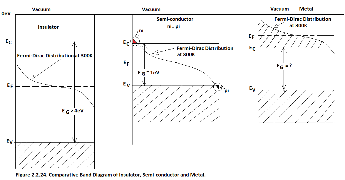
2.2.3. distinction between insulator,semi-conductor and ... from www.quizover.com The fermi level does not include the work required to remove the electron from wherever it came from. At t=0 f(e) = 1 for e < ev f(e) = 0 for e > ec 7 at higher temperatures some of the electrons have been electric field: The probability of occupation of energy levels in valence band and conduction band is called fermi level. (15) and (16) be equal at all temperatures, which yields the following expression for the position of the fermi level in an intrinsic semiconductor Intrinsic semiconductors are semiconductors, which do not contain impurities. Fermi energy of an intrinsic semiconductorhadleytugrazat. At absolute zero temperature intrinsic semiconductor acts as perfect insulator. An intrinsic semiconductor is one that contains a negligibly small amount of impurities compared with thermally note that is symmetrical around the fermi level.
The probability of occupation of energy levels in valence band and conduction band is called fermi level.
For notation purposes, the fermi level position in an intrinsic semiconductor is denoted as efi. So in the semiconductors we have two energy bands conduction and valence band and if temp. The surface potential yrsis shown as positive (sze, 1981). Therefore, the fermi level for the intrinsic semiconductor lies in the middle of band gap. Hence, using equation 4 and rearranging, the fermi. 4.2 dopant atoms and energy levels. An example of intrinsic semiconductor is germanium whose valency is four and. Where is the fermi level within the bandgap in intrinsic sc? Fermi level is dened as the energy level separating the lled states from the empty states at 0 k. Figure removed due to copyright restrictions. Room temperature intrinsic fermi level position). As the temperature increases free electrons and holes gets generated. „ position fermi energy level.
Carriers concentration in intrinsic semiconductor at equilibrium fermi level in semiconductor. 4.2 dopant atoms and energy levels.


0 Komentar